


![]()
Semiconductors have become ubiquitous, impacting every facet of our lives. From cars to refrigerators, computers, medical devices, and phones, the list goes on and on. But most people don’t really know how a semiconductor chip is made ─ it is a unique and fascinating process.
It all starts with grains of sand and from that silicon is extracted. The silicon is then purified, heated into a high-purity liquid, and crystallized into a solid rod or ingot. The ingots are then sliced into very thin wafers from 150-300mm in diameter. From this point on is technical wizardry!
Every Step of the Way ─ From Wafer Processing to Final Chip Configuration ─ There Are Plastic Components Involved
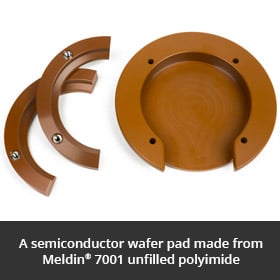
TriStar offers unique materials, like Meldin® 7001 polyimide, that are specifically engineered to withstand the 600°F temperatures encountered in vacuum deposition, oxidation, plasma etch, while also maintaining high levels of purity, thermal stability, and etch resistance. Additionally, Meldin® has high wear resistance, is non-galling, and chemical resistant, making it a perfect candidate for this very critical part of the process.
Further Downstream, There Are Many Other Plastics That Fit the Needs of These Unique Applications
Wafer cleaning is the step where the sliced and polished wafers are cleaned with strong chemicals. Plastic materials used for these processes must stand up to these chemicals for sustained periods. Critical components like cleaning tanks, lifting arms, and wafer holders call for known chemical-resistant materials such as PVDF, PPS, PEEK, PTFE, and other fluoropolymers.
CMP (Chemical-Mechanical Planarization) is the process where the surface of the wafer is precisely flattened to prepare it for photolithography. CMP uses chemical slurry and mechanical polishing to get the final finish required. Plastics employed in this aspect of processing include PPS, PEEK, and PET for retaining rings, transport trays, and other product handling components. They all have good chemical resistance, wear and abrasion resistance and are non-galling to the wafers.
The remaining steps include dicing, lead attachment, encapsulation, and final testing of the chips and packaging. Each stop along the way requires just the right material solution.
For Semiconductors, Specialized Materials and Careful Selection is Critical ─ TriStar Can Help
TriStar’s engineering team has decades of combined experience with high-performance plastics and can help you determine not only the right material, but also assist in determining the most cost-effective way to make your part. All with the end goal of improving your product performance and service life. If you’d like to hear more, we encourage you to reach out.