


From cars to computers to medical devices, today’s world is built on semiconductors. The TriStar team has gotten to know this industry up close in our work with Meldin 7001 (used for components in plasma deposition equipment), and we created this blog to provide a high-level overview of this incredibly sophisticated industry.
What raw materials are used to manufacture semiconductor devices?
Semiconductors can be made from a variety of materials including germanium, gallium arsenide, and silicon. While different materials may be employed in specialized applications, silicon has become the prototypical choice for modern electronic devices, and in many cases synonymous with semiconductor chips in general. Silicon ingots, the raw inputs of the chip manufacturing process, are manufactured by heating sand into a high-purity liquid which is then solidified through a crystallization process.
The Chip Manufacturing Process
Modern semiconductor device manufacturing is a highly complicated process that requires dozens of specialized processes, unique pieces of equipment, and extreme purity and precision. While documenting all of these processes is beyond the scope of this blog, the main steps outlined below provide an instructive overview of how raw silicon wafers are transformed into electronic devices with ever-growing performance potential.
Step 1: Initial Wafer Manufacturing and Preparation
Semiconductor chips are comprised of multiple layers of complex structures stacked onto a silicon wafer. To prepare for the manufacturing of these complex functional layers, raw silicon ingots must be sliced into thin wafers. These slices will exhibit substantial roughness and surface imperfections and must be polished before further processing. Each wafer contains many different individual chips, and overall wafer size plays a key role in determining how many chips can be manufactured in parallel using the same wafer.
Step 2: Wafer Oxidation
The oxidation process involves applying oxygen and water vapor to the wafer to form an oxide film. This film functions as an insulating layer and helps protect the surface of the wafer during subsequent processing.
Step 3: Photolithography
In this process, the fundamental pattern of a device’s integrated circuit is imprinted onto a wafer. First, a photo-resistive material (“photoresist”) is applied to the wafer. A glass substrate with an image of the desired circuit structure is then temporarily applied over this photoresist material. This image is transferred through the application of UV light, much like developing a photo—the glass substrate masks the photoresist layer, only allowing light to react and harden the photoresist in the desired pattern.
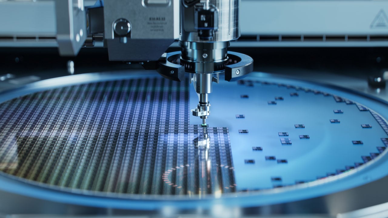
Step 4: Etching, Plasma Deposition, and Ionic Implantation
In this step, excess materials are removed from the photolithographed wafer so that only the desired chip structure remains. Gases (“dry etching”) or liquid chemicals (“wet etching”) are used to expose the final microstructure. In short, etching chemicals remove material that is not still protected by hardened photoresist after the lithography process.
Before the next phase begins, the lithography and etching processes are typically conducted several times to create more complex structures on a wafer in layers. Thin layers of insulating or conducting film (only a few nanometers thick) must be applied extremely precisely between each layer, using a plasma-based process known as “deposition,” to ensure that only desired connections between layers are created. We take a closer look at plasma deposition in our blog post here.
Finally, raw silicon wafers are not yet conductive. An ion implantation process effectively embeds impurities in the wafer to make the wafer conductive.
Step 5: Metal Wiring and Interconnection
Now, a thin metal film is applied to the microstructures created during the previous manufacturing processes. This metal interconnection ensures that signals can be passed between the various electronic structures underneath.
Step 6: Electrical Die Sorting
Because the semiconductor manufacturing process is so precise and demanding, even leading chip manufacturers employing the most advanced techniques and equipment on earth experience some rate of defective chips on each wafer. Optimizing the overall manufacturing process is critical to reducing defects and increasing yield—a critical operational variable for semiconductor manufacturers. In the electrical die-sorting process, chips are tested, and defective chips are marked for discarding prior to packaging.
Step 7: Packaging
In this final step, semiconductor wafers assume the form of the individual chips that consumers are likely to be familiar with. Wafers are cut into individual chips and packaged into materials that provide insulation, protection from the elements, and connection points to pass current to external devices. Contact points of semiconductor chips are bonded to PCB boards and wired to the board’s substrate.
Packaged chips are exposed to an intense battery of thermal and electrical tests to filter out defective components and rate the performance potential of successfully manufactured chips.
Learn More About Meldin® 7001 Components for Plasma Deposition Equipment
Advanced processes like plasma etching and deposition require extreme conditions that can rapidly degrade consumable components like screws and wafer handling rings. Meldin® 7001 offers the proven ability to stand up to these conditions, boosting component life while offering lower costs compared to competitor materials like Vespel® SP-1*. Learn more in our guide here.

*Vespel® is a registered trademark of DuPont Specialty Products USA, LLC.