


“The semiconductor industry is booming, with expected average annual growth of 6 to 8 percent through 2030 and yearly revenues forecasted to reach $1 trillion. The industry will have to double semiconductor production to keep pace with future demand, but most fabrication plants, commonly called fabs, are already operating at capacity. To increase supply, many companies have announced plans to build new fabs and some are already in the construction phase. And in a coordinated push to achieve a microelectronics resurgence, the United States is becoming a hot spot for fab construction.”
—McKinsey Report on Semiconductor Fab Construction Challenges in the United States
The semiconductor industry in the United States is booming. After decades of ceding global market share to chip manufacturers overseas, private and public sector leaders alike have come to view boosting domestic chip manufacturing as a strategic priority. Chip shortages have already cost the automotive industry alone over $200 billion in revenue, laying bare the vulnerabilities of global semiconductor supply chains that had become increasingly reliant on a small handful of suppliers. The CHIPS Act alone has injected over $50 billion in new funding, and a huge wave of new construction is underway, with a total of 18 new manufacturing facilities expected to be under construction in the United States by the end of 2023.
Semiconductors manufactured in the United States now account for only about 12 percent of the global total, down from 37 percent 30 years ago. Source.
As US chip manufacturers seek to scale up, improve efficiency, and bring down costs, leveraging advanced materials will be critical to addressing the unique engineering requirements of advanced semiconductor manufacturing equipment. The components employed inside the plasma deposition chambers instrumental to chip production provide an instructive example.
 As we explore throughout this guide, this manufacturing process involves extreme conditions for consumable components. Historically, Vespel® SP-1* has been the only widely available choice for these applications. Manufacturers who needed high-temperature, high-performance polymer materials with exceptional dimensional strength were faced with a narrow market of high-cost solutions—and limited choice.
Today, Meldin® 7001, a high-performance polyimide, offers a proven alternative that can match or exceed Vespel®’s performance characteristics, improving component lifespan in plasma deposition applications at an extremely competitive price point.
*Vespel® is a registered trademark of DuPont Specialty Products USA, LLC.
TriStar Plastics is proud to partner with Saint-Gobain as the exclusive North American distributor of Meldin® products. We have seen up close how these materials can help address incredibly tough challenges, and we are excited to offer them to our customers while supporting them with our value-added approach to materials engineering.
In this guide, we take a deeper dive into Meldin® 7001, its properties, and why it can offer exceptional value for in-chamber plasma deposition components.
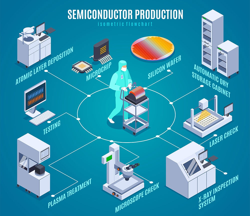
Unique Challenges for Materials Used in Semiconductor Manufacturing Equipment
 Semiconductor fabrication facilities (fabs) depend on a complex array of specialized machinery manufactured by a variety of OEMs to execute the dozens of distinct processes that go into transforming a silicon wafer into a finished chip with microstructures that can range down to the scale of just a few nanometers—thousands of times smaller than a grain of sand.
Some of the most important parts of this highly complex process include:
- Wafer Oxidation: oxygen and water vapor are applied to the wafer to form an oxide film which functions as an insulating layer and helps protect the surface of the wafer during subsequent processing.
- Photolithography: The image of an integrated circuit is transferred through the application of UV light—much like developing a photo—using a glass substrate and photosensitive material.
- Etching, Plasma Deposition, and Ionic Implantation: Excess materials are removed from the photolithographed wafer so that only the desired chip structure remains. Gases (“dry etching”) or liquid chemicals (“wet etching”) are used to expose the final microstructure.
The lithography and etching processes are typically conducted several times to create more complex structures on a wafer in layers. Thin layers of insulating or conducting film (only a few nanometers thick) must be applied extremely precisely between each layer, using a plasma-based process known as “deposition,” to ensure that only desired connections between layers are created. Finally, raw silicon wafers are not yet conductive. An ion implantation process effectively embeds impurities in the wafer to make the wafer conductive. - Metal Wiring and Interconnection: A thin metal film is applied to the microstructures created during the previous manufacturing processes to ensure that signals can be passed between the various electronic structures underneath.
- Electrical Die Sorting: In the electrical die-sorting process, chips are tested, and defective chips are marked for discarding prior to packaging.
- Packaging: Wafers are cut into individual chips and packaged into materials that provide insulation, protection from the elements, and connection points to pass current to external devices. Contact points of semiconductor chips are bonded to PCB boards and wired to the board’s substrate.
For a deeper look at the semiconductor manufacturing process, please see our blog post here.
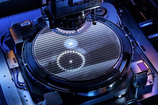
These processes must be repeated with extreme precision to create the multilayered structures employed in today’s chip designs. Even minute particle impurities can cause interference, refraction, and various other chemical defects at various points throughout the semiconductor manufacturing process. The combined need for high-purity materials and the need to stand up to extreme manufacturing conditions create unique challenges for the consumable components used in semiconductor manufacturing equipment. The plasma deposition process provides an instructive example.
Key Challenges for Plasma Deposition Components
Certain components in plasma deposition equipment are exposed directly to the extreme environment of a plasma deposition chamber. Prototypical examples are the components such as screws and wear rings used to hold silicon wafers in place during the plasma deposition process. The materials used in these components must hold up to extreme conditions without compromising the manufacturing process.
- Typical plasma deposition temperatures range up to 400°C, and materials employed in-chamber must be able to resist deformation at repeated cycling up to these high temperatures.
- Materials used for in-chamber components must be exceptionally pure and resistant to outgassing during the deposition process. Particles, water vapor, and other contaminants emitted at high temperatures can directly reduce yield.
- Most polymers exhibit low levels of metal material as an inherent result of the machinery used in the manufacturing process. However, these ionic contaminants must be eliminated for the materials used in plasma deposition chambers. Even trace amounts of contaminants risk effectively shorting out the microstructures employed on silicon chips.
- Materials employed in in-chamber components must also be able to withstand the caustic chemicals employed in the chip manufacturing process.
- Components must be made from materials that offer strong dielectric insulation properties.
The ability of costly consumable components such as wafer handling rings to withstand repeated exposure to the plasma deposition process has important implications for operating costs and maintenance downtime when a replacement is required.
Aftermarket Components Are Critical to Maximizing Long-Term ROI for Plasma Deposition Equipment
The cost of replacement consumable parts is a critical determining factor for the long-term cost structure of plasma deposition equipment. While parts will typically need to be purchased from the OEM for the duration of the warranty, OEM components are often supplied at a substantial cost premium compared to aftermarket alternatives. For this reason, a warranty’s expiration may create new opportunities for savings using aftermarket parts—if they can stand up to the challenging requirements of the plasma deposition processes employed in the semiconductor industry.
By providing a cost-effective material for replacing high-purity components for plasma deposition, Meldin® 7001 can help extend the life of capital-intensive semiconductor manufacturing equipment, boosting ROI.
What is Meldin® 7001?
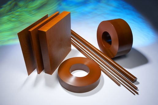 Meldin® 7001 is the base unfilled resin formulation of the Meldin® 7000 series of polyimides. These thermosetting plastics exhibit no glass transition temperature or melting point, making them ideal for high-temperature applications, dielectric applications, and high-purity applications, like the plasma deposition equipment used in semiconductor manufacturing.
About the Meldin® Family
Meldin® is a family of high-performance polymers manufactured by Saint-Gobain, a world leader in materials engineering. Meldin® family materials are available in a number of product lines and formulations, which can offer combinations of extreme temperature resistance, exceptional dimensional stability, and wear resistance capable of delivering outstanding service life in extremely hazardous environments. You will find Meldin® materials everywhere from inside jet engines to the vacuum of space.
The Meldin® family of materials was initially formulated by Furon-Dixon in the late 1960’s as one of the first commercially available pure thermoset polyimides. Now owned by Saint-Gobain, Meldin® materials have advanced alongside new developments in polyimide chemistry for many years.
For a broader look at the Meldin® family of materials, please see our guide here.
About Meldin® 7000 Series Polyimides
Polyimide materials have their roots in research conducted by NASA for the early space program, where they were developed for use as a heat shield material. While originally prohibitively costly for civilian applications, Meldin® has been developed over time into a leading material for high-temperature applications. The Meldin® 7000 series’ temperature tolerance exceeds that of materials like Torlon® and PEEK, which break down at high temperatures. And its physical strength exceeds that of high-temperature alternatives such as PTFE. We take a deeper look at what makes the Meldin® 7000 series different in our blog post here.
As part of the Meldin® 7000 family, Meldin® 7001 offers:
- Excellent resistance to high-energy radiation.
- Very low outgassing in a vacuum and low ionic contamination.
- Good chemical resistance to a variety of chemicals and hydrocarbons.
- Fully stable in continuous operating temperatures up to 700°F and intermittent temperatures up to 900° Formulations like Meldin® 7001 also exhibit excellent properties at cryogenic temperatures.
- The ability to retain stability in the face of repetitive thermal cycling. Testing demonstrates that Meldin® 7000 series materials exhibit less than .04% variation from their original dimension after cycling from 73°F to 500°F over a 2-day period.
- Excellent dielectric and thermal insulation properties.
- Inherently good wear and friction qualities, with high PV ratings.
The central limitation of these materials is that they must not be exposed to steam or water. Meldin® is fabricated using polycondensation, a process that involves a condensation reaction that releases water as constituent monomers are combined. Hot moisture will effectively “re-condensate” the material, causing it to fall apart.
Competitive Advantages of Meldin® 7001 Components in Plasma Deposition Applications
Whether specified in OEM designs or used in after-market parts, Meldin® 7001 offers all of the attributes of competitive products needed to perform in demanding in-chamber plasma deposition applications at a compelling price point.
In the past, Meldin® components were proposed for plasma deposition applications but failed to provide the required performance characteristics in testing. These earlier formulations were too brittle and exhibited too much outgassing for use in plasma deposition chambers.
The “new Meldin®”, however, has been re-engineered by Saint-Gobain to equal and in many cases surpass the characteristics offered by Vespel®.
- Meldin® 7001 is manufactured using a hot isostatic press (HIP) process, identical to that used by Vespel® SP-1. Older formulations of Meldin® used a compression molding process. An isostatic process provides for greater uniformity. Because isostatic pressure is applied from the same direction, the resultant material exhibits defined structures with excellent cross-sectional stability.
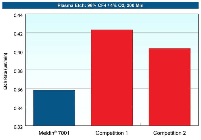
- Meldin® 7001 offers 10-14% better plasma etch resistance compared to competitors, driving longer component life and reduced equipment downtime.
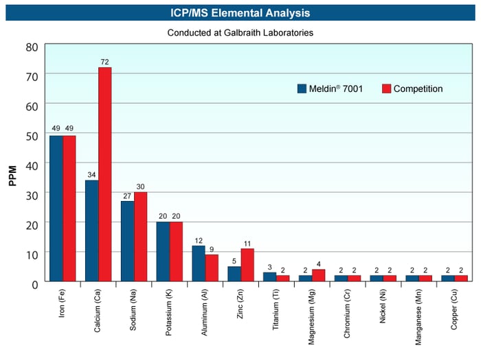
- Meldin® 7001 exhibits equal and often superior ionic purity compared to Vespel® SP-1, essential for limiting interference in plasma deposition chambers to boost yield.
- Third-party testing labs have used outgassing tests conducted per ASTM E595 at 125⁰C to verify that Meldin® has 35% lower total mass loss and 11% lower vapor regain compared to Vespel®.
How do Meldin® 7001’s thermal properties drive improved lifespan in plasma deposition applications?
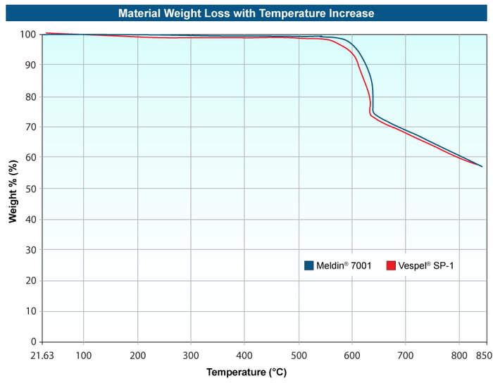
Meldin® 7001 offers exceptional thermal oxidative stability (the ability of a material to sustain its properties through heat-driven aging). This attribute minimizes weight loss at high temperatures and pressures compared to traditional polyimide component materials. The stability demonstrated in the graph below leads directly to extended components lifespan and reduced maintenance needs.
As the data below demonstrate, the material starts to exhibit minimal weight loss only at temperatures over 500°C. For the high-purity requirements of plasma deposition, we suggest continuous use up to 316°C and intermittent use up to 482°C. Compared to competitor polyimides like Vespel® SP1, Meldin® 7001 burns away less quickly at extreme temperatures.
Additionally, Meldin® 7001 exhibits minimal creep under load, even at high temperatures. For Meldin® 7001, the additional creep at 100°C at both low and high pressure is less than 0.2%. Even at 300°C, Meldin® 7001 exhibits a very low creep, less than 0.4% at lower loads and under 0.9% at high loads.
Learn More About How to Leverage Meldin® 7001 to Improve Lifespan for Semiconductor Manufacturing Equipment
 We hope this guide has provided a useful look at why Meldin® 7001 can offer exceptional value for both OEM and aftermarket components used in plasma deposition equipment. In addition to competive pricing compared to the competiton, the improved lifespan of Meldin® components can help reduce part replacement costs in addition to maintenance costs due to downtime.
For a deeper look at our full range of Meldin® materials and their specifications, please refer to our interactive materials database here.
If you need help sourcing the right materials for your semiconductor manufacturing components, the TriStar team is here to help. We recognize that maximizing ROI for the costly components employed in plasma deposition processes is about more than simply picking the right material off the shelf. Our team can help ensure that the right materials are aligned to your unique application requirements.
Our team is dedicated to learning about the specific engineering challenges driving every client application. In our experience working with a huge variety of high-performance applications, this consultative engineering approach almost always pays off.
Meldin® is a registered trademark of Saint-Gobain Performance Plastics Corporation.
Vespel® is a registered trademark of DuPont Specialty Products USA, LLC.
Torlon® is a registered trademark of Solvay Advanced Polymers.